 | –≠–ª–µ–∫—Ç—Ä–æ–Ω–Ω—ã–π –∫–æ–º–ø–æ–Ω–µ–Ω—Ç: LTC1564 | –°–∫–∞—á–∞—Ç—å:  PDF PDF  ZIP ZIP |
1
LTC1564
10kHz to 150kHz
Digitally Controlled
Antialiasing Filter and 4-Bit P.G.A
s
4-Bit Digitally Controlled 8th-Order Lowpass Filter
≠ f
CUTOFF
Adjustable from 10kHz to 150kHz in 10kHz
Steps
≠ 100dB Attenuation at 2.5
◊
f
CUTOFF
s
4-Bit Digitally Controlled Programmable Gain
Amplifier
≠ G = 1 to 16 in 1V/V Steps
s
Miniature 16-Pin SSOP Package
s
No External Components
s
122dB Total System Dynamic Range
s
Rail-to-Rail Input and Output Range
s
2.7V to 10V Operation
s
Low Noise Mute Mode
s
Low Power Shutdown Mode
s
Antialias or Reconstruction Filtering
s
DSP Systems
s
Communications Systems
s
Scientific Instruments
s
High Resolutions (16 Bits to 20 Bits)
s
Processing Signals Buried in Noise
s
Audio Signal Processing
s
Programmable Data Rates
s
Automatic Gain Control (AGC)
s
Single Part Replacing Multiple Filters
Low Noise Programmable Filter with Variable Gain
, LTC and LT are registered trademarks of Linear Technology Corporation.
The LTC
Æ
1564 is a new type of continuous time filter for
antialiasing, reconstruction and other band-limiting appli-
cations. No other analog components or filter expertise are
needed to use it. There is one analog input pin and one
analog output pin. The cutoff frequency (f
C
) and gain are
programmable while the shape of the lowpass response is
fixed. A latching digital interface stores f
C
and gain settings
or it can be bypassed for control directly from the pins. The
LTC1564 operates from 2.7V to 10V total (single or split
supplies) and comes in a 16-pin surface mount SSOP.
The LTC1564 is a rail-to-rail high resolution 8th-order
lowpass filter with two stopband notches, giving approxi-
mately 100dB attenuation at 2.5 times the passband cutoff
frequency f
C
(a de-facto standard for DSP front ends).
Signals with low or variable levels can be normalized with
the built-in variable gain that reduces input-referred noise
with increasing gain for a typical dynamic range (maxi-
mum signal level to minimum noise) of 122dB (20 equiva-
lent bits) with 20kHz f
C
and 118dB at 100kHz f
C
on a
±
5V
supply.
Other frequency-response shapes can be provided upon
request. Please contact LTC Marketing.
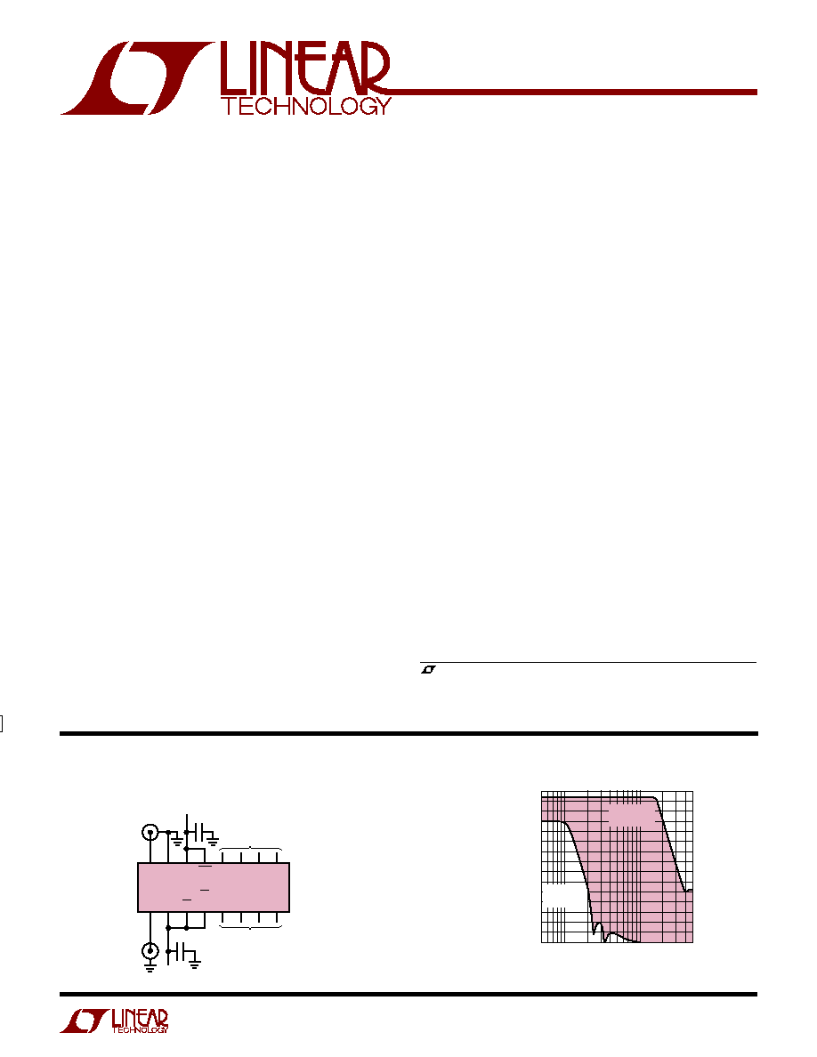
IN AGND V
+
RST G3
LTC1564
G2
G1
G0
OUT V
≠
1
2
3
4
5
6
7
1564 TA01
8
16
15
14
13
12
11
GAIN CODE
FREQUENCY CODE
V
+
AND V
≠
SUPPLIES CAN BE FROM
1.35V TO 5.25V EACH
TIE F AND G PINS TO V
+
OR V
≠
TO
SET FREQUENCY AND GAIN
DYNAMIC RANGE 118dB TO 122dB
AT
±
5V DEPENDING ON FREQUENCY CODE
0.1
µ
F
V
+
10
9
EN
CS/
HOLD F3
F2
F1
F0
0.1
µ
F
ANALOG
OUT
ANALOG
IN
V
≠
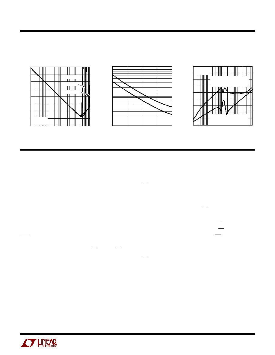
LTC1564 Programmable Range
FREQUENCY (kHz)
5
GAIN (dB)
10
100
500
1564 TA02
10
30
20
0
≠10
≠20
≠30
≠40
≠50
≠60
≠70
≠80
≠120
≠110
≠100
≠90
f
C
= 10kHz
GAIN = 1V/V
f
C
= 150kHz
GAIN = 16V/V
FEATURES
DESCRIPTIO
U
APPLICATIO S
U
TYPICAL APPLICATIO
U
2
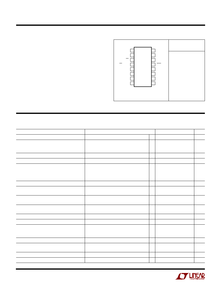
LTC1564
G PACKAGE
16-LEAD PLASTIC SSOP
1
2
3
4
5
6
7
8
TOP VIEW
16
15
14
13
12
11
10
9
OUT
V
≠
EN
CS/HOLD
F3
F2
F1
F0
IN
AGND
V
+
RST
G3
G2
G1
G0
PARAMETER
CONDITIONS
MIN
TYP
MAX
UNITS
Total Supply Voltage
2.7
10.5
V
Supply Current
V
S
=
±
1.35V, V
IN
= 0V
q
15
17
mA
V
S
=
±
2.375V, V
IN
= 0V
q
16
18.5
mA
V
S
=
±
5V, V
IN
= 0V
q
22
25
mA
Output Voltage Swing
R
L
= 10k to 0V
q
4.5
4.65
V
P-P
Output Short-Circuit Current
V
S
=
±
5V
q
±
10
mA
DC Offset Voltage Magnitude (Referred to Input)
Gain = 1, 0
∞
C to 70
∞
C
q
3
13
mV
Gain = 1, ≠ 40
∞
C to 85
∞
C
q
3
16
mV
Gain = 10, 0
∞
C to 70
∞
C
q
1
5
mV
Gain = 10, ≠ 40
∞
C to 85
∞
C
q
1
6
mV
DC AGND Reference Voltage
V
S
= Single 5V Supply
2.5
V
Passband Gain
f
C
= 50kHz, f
IN
= 10kHz, Gain = 1
q
≠ 0.1
0.3
0.8
dB
f
C
= 50kHz, f
IN
= 10KHz, Gain = 16
q
23.5
24.2
25.3
dB
Passband Ripple
f
C
= 10kHz, 0
f
IN
9kHz (Notes 2, 3)
q
≠0.5
0.5
dB
f
C
= 150kHz, 0
f
IN
135kHz (Notes 2, 3)
q
≠ 0.6
1.6
dB
Roll Off at Cutoff Frequency (f
C
) (Note 3)
f
C
= 10kHz (F = 0001)
q
≠1.2
≠0.7
≠0.3
dB
f
C
= 150kHz (F = 1111)
q
≠1.5
≠0.5
0.6
dB
Roll Off at 2f
C
(Note 3)
f
C
= 10kHz
q
≠65
≠62
≠59
dB
Roll Off at 2.5f
C
(Note 3)
f
C
= 10kHz
≠99
dB
Wideband Noise (Referred to Input)
BW = 20kHz, f
C
= 10kHz, Gain = 1
33
µ
V
RMS
BW = 20kHz, f
C
= 10kHz, Gain = 16
2.5
µ
V
RMS
BW = 200kHz, f
C
= 100kHz, Gain = 1
50
µ
V
RMS
Total Harmonic Distortion
f
C
= 100kHz, f
IN
= 10kHz, V
IN
= 1V
RMS
≠ 86
dB
Input Impedance
Gain = 1, DC V
IN
= 0V
10
k
Gain = 16, DC V
IN
= 0V
625
Output Impedance
f
C
= 10kHz, f = 10kHz
30
Mute State (F = 0000) Gain
F = 0000, f
IN
= 20kHz, V
IN
= 1V
RMS
≠103
dB
(Note 1)
Total Supply Voltage (V
+
to V
≠
) .............................. 11V
Input Voltage ............................. V
+
+ 0.3V to V
≠
≠ 0.3V
Output Short-Circuit Duration .......................... Indefinite
Operating Temperature Range
LTC1564C .............................................. 0
∞
C to 70
∞
C
LTC1564I .......................................... ≠ 40
∞
C TO 85
∞
C
Storage Temperature Range ................. ≠ 65
∞
C to 150
∞
C
Lead Temperature (Soldering, 10 sec).................. 300
∞
C
ORDER PART
NUMBER
LTC1564CG
LTC1564IG
T
JMAX
= 125
∞
C,
JA
= 130
∞
C/ W
The
q
denotes specifications that apply over the full operating temperature
range, otherwise specifications are at T
A
= 25
∞
C. V
S
=
±
2.375V, f
C
= 10kHz, gain = 1, R
L
= 10k, unless otherwise noted.
ABSOLUTE AXI U RATI GS
W
W
W
U
PACKAGE/ORDER I FOR ATIO
U
U
W
ELECTRICAL CHARACTERISTICS
Consult factory for parts specified with wider operating temperature ranges.
3
LTC1564
PARAMETER
CONDITIONS
MIN
TYP
MAX
UNITS
Mute State Output Noise
F = 0000, BW = 200kHz
5.4
µ
V
RMS
Shutdown Supply Current
V
S
=
±
1.35V, EN to V
+
45
75
µ
A
V
S
=
±
1.35V, EN to V
+
q
150
µ
A
V
S
=
±
2.375V, EN to V
+
100
150
µ
A
V
S
=
±
2.375V, EN to V
+
q
180
µ
A
V
S
=
±
5V, EN to V
+
(Note 4)
175
µ
A
Digital Input "High" Voltage
V
S
=
±
1.35V
1.08
V
V
S
=
±
2.375V
1.90
V
V
S
=
±
5V
4.50
V
Digital Input "Low" Voltage
V
S
=
±
1.35V
≠1.08
V
V
S
=
±
2.375V
≠1.90
V
V
S
=
±
5V
0.50
V
Digital Input Pull-Up or Pull-Down Current (Note 5)
V
S
=
±
1.35V
q
3.5
6
µ
A
(Digital Inputs Other than EN)
V
S
=
±
5V
q
13
20
µ
A
Digital Input Pull-Up Current (EN Input)
V
S
=
±
1.35V
q
1
2
µ
A
V
S
=
±
5V
q
10
20
µ
A
The
q
denotes specifications that apply over the full operating temperature
range, otherwise specifications are at T
A
= 25
∞
C. V
S
=
±
2.375V, f
C
= 10kHz, gain = 1, R
L
= 10k, unless otherwise noted.
ELECTRICAL CHARACTERISTICS
Note 1: Absolute Maximum Ratings are those values beyond which the life
of the device may be impaired.
Note 2: Response is tested in production at discrete frequencies f
IN
of 0.1,
0.5, 0.8 and 0.9 times f
C
.
Note 3: Relative to gain at 0.1f
C
.
Note 4: All digital inputs driven rail-to-rail. When driving digital inputs with
0V and 5V levels, the shutdown current will increase to 3.5mA (typ).
Note 5: Each digital input includes a small positive or negative current
source to float the CMOS input to V
+
or V
≠
potential if it is unconnected.
The table shows the current due to this source when the input is driven at
the supply voltage opposite from the float potential. Pins CS/HOLD, F3, F2,
F0 and G3 to G0 float to the V
≠
voltage, pins RST, EN and F1 to the V
+
voltage. See "Floatable Digital Inputs" in Applications Information section.
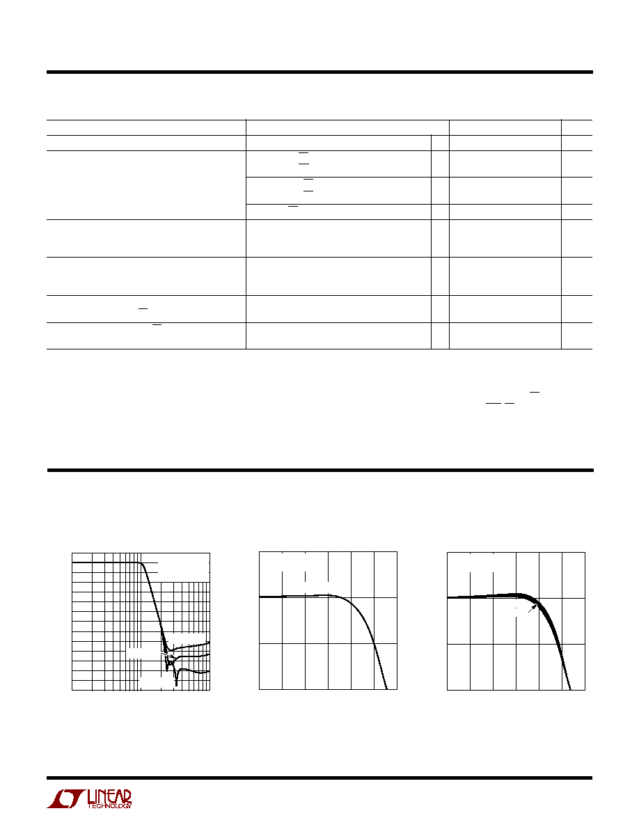
TYPICAL PERFOR A CE CHARACTERISTICS
U
W
Overall Frequency Response
(Frequency Scales Normalized to f
C
)
f
IN
/f
C
≠130
≠70
≠90
≠110
10
0
≠10
≠30
≠50
≠80
≠100
≠120
≠20
≠40
≠60
1564 G01
GAIN (dB)
0.1
10
1
f
C
= 10kHz
f
C
= 150kHz
f
C
= 50kHz
V
S
= SINGLE 5V
UNITY GAIN
(G CODE 0000)
FREQUENCY (kHz)
5
≠10
GAIN (dB)
≠5
0
5
6.25
7.5
8.75
10
1564 G02
11.25
12.5
≠40
∞
C, 25
∞
C, 85
∞
C
f
C
= 10kHz
SINGLE 5V SUPPLY
FREQUENCY (kHz)
50
≠10
GAIN (dB)
≠5
0
85
∞
C
5
62.5
75
87.5
100
1564 G03
112.5
125
f
C
= 100kHz
SINGLE 5V SUPPLY
≠40
∞
C
25
∞
C
Roll-Offs Over Temperature
(f
C
= 10kHz)
Roll-Offs Over Temperature
(f
C
= 100kHz)
4
LTC1564
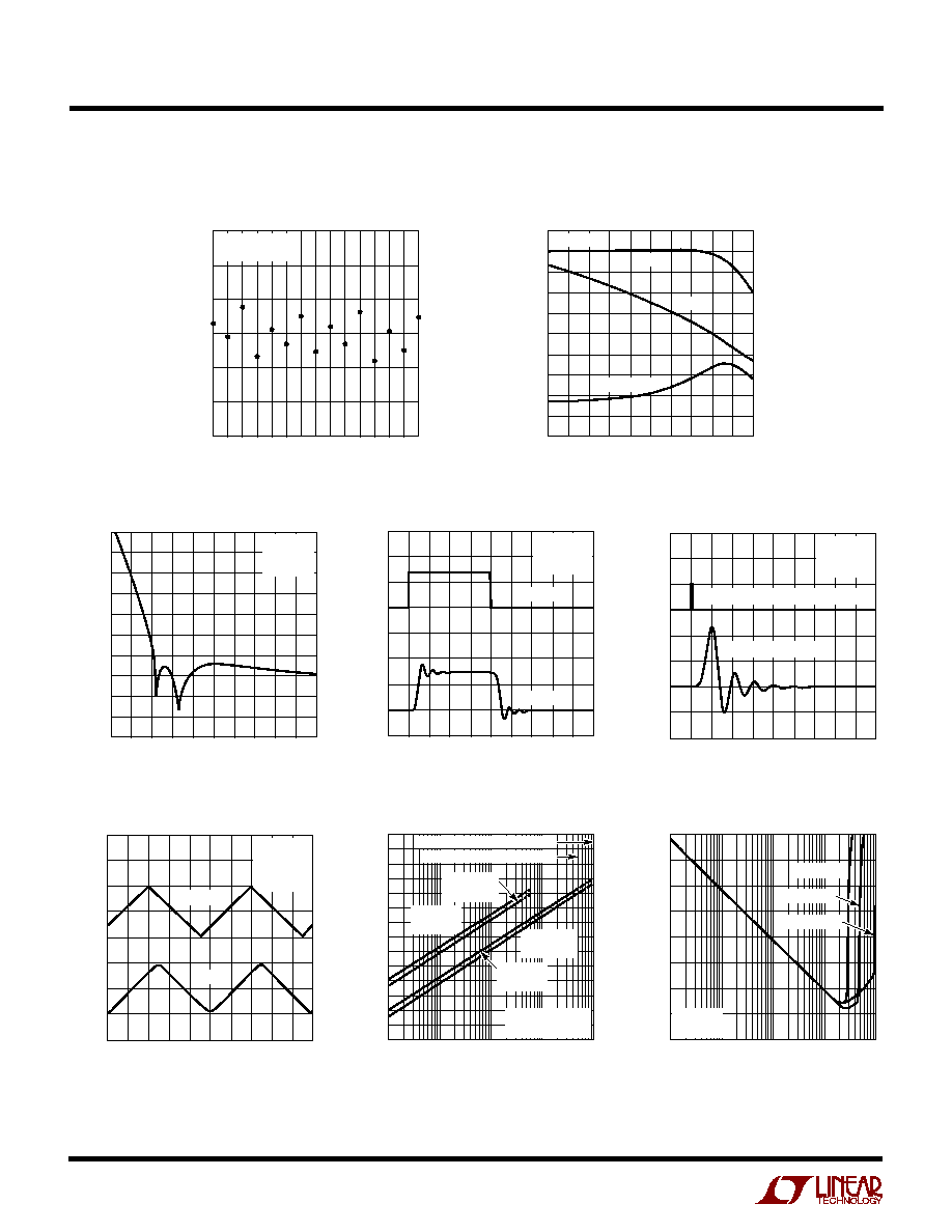
TYPICAL PERFOR A CE CHARACTERISTICS
U
W
Detail of Stopband Response
Passband Gain, Phase
and Group Delay
f
C
(kHz)
10
GAIN (dB)
≠0.50
≠0.25
0
70
110
1564 G04
≠0.75
≠1.00
30
50
90
130
150
≠1.25
≠1.50
V
S
= SINGLE 5V
T
A
= 25
∞
C
FREQUENCY (kHz)
15
GAIN (dB)
≠80
≠60
≠40
55
1564 G05
≠100
≠120
≠90
≠70
≠50
≠110
≠130
≠140
25
35
45
65
f
C
= 10kHz
V
S
=
±
5V
T
A
= 25
∞
C
FREQUENCY (kHz)
2
GAIN (dB)
PHASE (DEGREES)
≠15
≠5
5
10
1546 G06
≠25
≠35
≠20
≠10
0
≠30
≠40
≠45
≠270
≠90
90
≠450
≠630
≠360
≠180
0
≠540
≠720
≠810
DELAY (
µ
s)
300
400
500
200
100
250
350
450
150
50
0
4
6
8
12
GAIN
f
C
= 10kHz
PHASE
GROUP DELAY
Passband Roll-Off at f
IN
= f
C
vs f
C
2V/DIV
1564 G07
200
µ
s/DIV
OUTPUT
f
C
= 10kHz
UNITY GAIN
V
S
=
±
5V
INPUT
100
µ
s/DIV
1564 G08
INPUT, 1V/DIV (PULSE WIDTH 10
µ
s)
OUTPUT, 100mV/DIV
f
C
= 10kHz
UNITY GAIN
V
S
=
±
5V
Rectangular Pulse Response
Short-Pulse Response
Triangular-Wave Time Response
SNR vs Input Voltage
THD + Noise vs Input Voltage
(f
C
= 10kHz)
200
µ
s/DIV
5V/DIV
1564 G09
f
C
= 10kHz
f
IN
= 1kHz
UNITY GAIN
V
S
=
±
5V
INPUT
OUTPUT
INPUT VOLTAGE (V
P-P
)
≠80
(THD + NOISE)/SIGNAL (dB)
≠60
≠50
≠30
≠20
0.001
0.1
1
10
1564 G11
≠100
0.01
≠40
≠70
≠90
3V SUPPLY
5V SUPPLY
±
5V SUPPLY
f
C
= 10kHz
f
IN
= 1kHz
INPUT VOLTAGE (V
P-P
)
30
10
SIGNAL/NOISE (dB)
50
70
90
110
0.001
0.1
1
10
1564 G10
0
0.01
140
130
20
40
60
80
100
120
GAIN = 16
f
C
= 20kHz
GAIN = 1
f
C
= 100kHz
GAIN = 1
f
C
= 20kHz
GAIN = 16
f
C
= 100kHz
LIMIT FOR 5V TOTAL SUPPLY
LIMIT FOR 10V TOTAL SUPPLY
PASSBAND INPUT
(f
IN
< f
C
)
5
LTC1564
TYPICAL PERFOR A CE CHARACTERISTICS
U
W
U
U
U
PI FU CTIO S
OUT (Pin 1): Analog Output. In normal filtering, this is the
output of an internal operational amplifier and is capable
of swinging essentially to any voltage between the power
supply rails (that is, between V
+
and V
≠
). This output is
designed to drive a nominal load of 5k and 50pF. For
lowest signal distortion it should be loaded as lightly as
possible. The output can drive lower resistances than 5k,
but distortion may increase, and the output current will
limit at approximately
±
10mA. Capacitances higher than
50pF should be isolated by a series resistor of 500
to
preserve AC stability. In the Mute state (F code 0000 or
RST = 0), the output operates as in normal filtering but the
gain from the IN pin becomes zero and the output noise is
reduced. In the shutdown state (EN = 1 or EN open
circuited), most of the circuitry in the LTC1564 shuts off
and the OUT pin assumes a high impedance state.
V
≠
, V
+
(Pins 2, 14): Power Supply Pins. The V
+
and V
≠
pins should be bypassed with 0.1
µ
F capacitors to an
adequate analog ground plane using the shortest possible
wiring. Electrically clean supplies and a low impedance
ground are important for the high dynamic range and high
stopband suppression available from the LTC1564 (see
further details under AGND). Low noise linear power
supplies are recommended. Switching supplies are not
recommended because of the inevitable risk of their
switching noise coupling into the signal path, reducing
dynamic range.
EN (Pin 3): CMOS-Level Digital Chip Enable Input. Logic 1
or open circuiting this pin causes a shutdown mode with
reduced supply current. The active circuitry in the LTC1564
shuts off and its output assumes a high impedance state.
If F and G bits are latched (CS/HOLD = 1) during the
shutdown state, the latch will retain its contents.
A small pull-up current source at the EN input causes the
LTC1564 to be in shutdown state if the EN pin is left open.
Therefore, the user must connect the EN pin to logic 0 (V
≠
or optionally 0V with
±
5V supplies) for normal filter
operation.
CS/HOLD (Pin 4): CMOS-Level Digital Enable Input for the
Latch Holding F and G Bits. Logic 0 makes the latch
transparent so that the F and G inputs directly control the
filter's cutoff frequency and gain. Logic 1 holds the last
values of these inputs prior to the transition. This pin floats
to logic 0 (V
≠
) when open circuited because of a small
current source (see Electrical Characteristics, Note 5).
F3, F2, F1, F0 (Pins 5, 6, 7, 8): CMOS-Level Digital
Frequency Control ("F Code") Inputs. F3 is the most
significant bit (MSB). These pins program the LTC1564's
cutoff frequency f
C
through the internal latch, which
THD + Noise vs Input Voltage
(f
C
= 100kHz)
INPUT VOLTAGE (V
P-P
)
≠80
(THD + NOISE)/SIGNAL (dB)
≠60
≠50
≠30
≠20
0.001
0.1
1
10
1564 G12
≠100
0.01
≠40
≠70
≠90
3V SUPPLY
5V SUPPLY
±
5V SUPPLY
f
C
= 100kHz
f
IN
= 10kHz
BASEBAND GAIN SETTING
2
1
10
100
4
8
1564 G13
INPUT-REFERRED NOISE (
µ
V
RMS
)
1
16
f
C
= 100kHz
f
C
= 10kHz
FREQUENCY (Hz)
≠60
GAIN (dB)
≠40
≠30
≠10
10
0.1k
10k
100k
1M
1564 G14
≠80
1k
≠20
≠50
≠70
0
f
C
= 10kHz
V
S
=
±
2.5V
NEGATIVE SUPPLY
V
+
SUPPLY BYPASS = 0.1
µ
F
V
≠
SUPPLY BYPASS = NONE
POSITIVE SUPPLY
V
+
SUPPLY BYPASS = NONE
V
≠
SUPPLY BYPASS = 0.1
µ
F
Noise vs Frequency
and Gain Settings
Power Supply Rejection
vs Frequency
6
LTC1564
U
U
U
PI FU CTIO S
passes the bits directly when the CS/HOLD input is at logic
0. When CS/HOLD changes to logic 1, the F pins cease to
have effect and the latch holds the previous values. The F
code controls the filter's cutoff frequency f
C
in 10kHz steps
up to 150kHz, as summarized in Table 1.
Table 1
F3
F2
F1
F0
NOMINAL F
C
(AT OUTPUT OF INTERNAL LATCH)
(CUTOFF FREQUENCY)
0
0
0
0
0 (Mute State: Filter Gain is Zero)
0
0
0
1
10kHz
0
0
1
0
20kHz
0
0
1
1
30kHz
0
1
0
0
40kHz
0
1
0
1
50kHz
0
1
1
0
60kHz
0
1
1
1
70kHz
1
0
0
0
80kHz
1
0
0
1
90kHz
1
0
1
0
100kHz
1
0
1
1
110kHz
1
1
0
0
120kHz
1
1
0
1
130kHz
1
1
1
0
140kHz
1
1
1
1
150kHz
Thus f
C
is proportional to the binary value of the F code.
Note that small current sources pull F1 to V
+
and F3, F2
and F0 to V
≠
when these pins are left unconnected (see
Electrical Characteristics, Note 5). This sets an F code
input of 0010 (2, in decimal form) by default, giving an f
C
of 20kHz in normal filtering operation, if CS/HOLD is logic
0 or is open circuited.
G0, G1, G2, G3 (Pins 9, 10, 11, 12): CMOS-Level Digital
Gain Control ("G Code") Inputs. G3 is the most significant
bit (MSB). These pins program the LTC1564's passband
gain through the internal latch, which passes the bits
directly when the CS/HOLD input is at logic 0. When
CS/HOLD changes to logic 1, the G pins cease to have
effect and the latch retains the previous input values. This
gain control is linear in amplitude: nominal passband gain
of the LTC1564 is the binary value of the G code, plus one
as shown in Table 2.
Note that small current sources pull the G pins to V
≠
when
these pins are left unconnected (see Electrical Character-
istics, Note 5). This sets a G code input of 0000 by default,
giving unity passband gain in normal filtering operation, if
CS/HOLD is logic 0 or is open circuited.
RST (Pin 13): CMOS-Level Asynchronous Reset Input.
Logic 0 on this pin immediately resets the internal F and G
latch to all zeros, regardless of the state of the CS/HOLD
pin or the F or G input pins. This causes the LTC1564 to
enter a mute state (powered but with zero signal gain)
because of the resulting F = 0000 command. Logic 1
permits the other pins to control F and G. This pin floats to
logic 1 (V
+
) when open circuited because of a small
current source (see Electrical Characteristics, Note 5). A
brief internal reset (shorter than the analog settling time of
the filter) also occurs when power is first applied.
NOMINAL
NOMINAL
G3
G2
G1
G0 PASSBAND GAIN
(VOLTS PEAK-TO-PEAK)
INPUT IMPEDANCE
(VOLT/VOLT) (dB)
DUAL 5V SINGLE 5V SINGLE 3V
(k
)
0
0
0
0
1
0
10
5.0
3.0
10
0
0
0
1
2
6.0
5
2.5
1.5
5
0
0
1
0
3
9.5
3.33
1.67
1.0
3.33
0
0
1
1
4
12
2.5
1.25
0.75
2.5
0
1
0
0
5
14.0
2
1
0.6
2
0
1
0
1
6
15.6
1.67
0.83
0.5
1.67
0
1
1
0
7
16.9
1.43
0.71
0.43
1.43
0
1
1
1
8
18.1
1.25
0.63
0.38
1.25
1
0
0
0
9
19.1
1.1
0.56
0.33
1.11
1
0
0
1
10
20.0
1.0
0.50
0.30
1
1
0
1
0
11
20.8
0.91
0.45
0.27
0.91
1
0
1
1
12
21.6
0.83
0.42
0.25
0.83
1
1
0
0
13
22.3
0.77
0.38
0.23
0.77
1
1
0
1
14
22.9
0.71
0.36
0.21
0.71
1
1
1
0
15
23.5
0.67
0.33
0.20
0.66
1
1
1
1
16
24.1
0.63
0.31
0.19
0.63
(AT OUTPUT OF INTERNAL LATCH)
MAXIMUM INPUT SIGNAL LEVEL
Table 2
7
LTC1564
AGND (Pin 15): Analog Ground. The AGND pin is at the
midpoint of an internal resistive voltage divider, develop-
ing a potential halfway between the V
+
and V
≠
pins, with
an equivalent series resistance to the pin of nominally 7k.
(In the shutdown state, analog switch FETs interrupt the
voltage-divider resistors and the AGND pin assumes a
high impedance.) AGND also serves as the internal half-
supply reference in the LTC1564, tied to the noninverting
inputs of all internal op amps and establishing the ground
reference voltage for the IN and OUT pins. Because of this,
very "clean" grounding is recommended, including an
U
U
U
PI FU CTIO S
LTC1564
DIGITAL GROUND PLANE
(IF ANY)
ANALOG
GROUND PLANE
1
SINGLE-POINT
SYSTEM GROUND
2
3
4
5
6
7
1564 F01
8
16
15
14
13
12
11
0.1
µ
F
V
+
10
9
0.1
µ
F
V
≠
Figure 1. Dual Supply Ground Plane Connection
LTC1564
DIGITAL GROUND PLANE
(IF ANY)
ANALOG
GROUND PLANE
1
SINGLE-POINT
SYSTEM GROUND
2
3
4
5
6
7
1564 F01
8
16
V
+
/2
REFERENCE
15
14
13
12
11
0.1
µ
F
1
µ
F
V
+
10
9
Figure 2. Single Supply Ground Plane Connection
analog ground plane surrounding the package. For dual
supply operation, this ground plane will be tied to the 0V
point and the AGND pin should connect directly to the
ground plane (Figure 1). For single supply operation, in
contrast, if the system signal ground is at V
≠
, the ground
plane should tie to V
≠
and the AGND pin should be AC-
bypassed to the ground plane by at least a 0.1
µ
F high
quality capacitor (at least 1
µ
F for best AC performance)
(Figure 2). As with all high dynamic range analog circuits,
performance in an application will reflect the quality of the
grounding.
Table 3. Summary of LTC1564 Digital Controls and Modes
EN
RST
CS/HOLD
F3
F2
F1
F0
G3
G2 G1
G0
FUNCTION
1
1
1
X
X
X
X
X
X
X
X
Shutdown Mode. Filter Disabled. Latch Holds F and G Inputs Present
when Last CS/HOLD = 0
1
1
0
X
X
X
X
X
X
X
X
Shutdown Mode. Filter Disabled. Latch Accepts F and G Inputs
1
0
X
X
X
X
X
X
X
X
X
Shutdown Mode. Filter Disabled. Latch Contents (F and G) Reset to All Zeros
0
1
0
0
0
0
0
X
X
X
X
Mute Mode. Filter Active, Zero Gain, Reduced Noise
0
0
X
X
X
X
X
X
X
X
X
Mute Mode. Filter Active, Zero Gain, Reduced Noise. Latch Contents
(F and G) Reset to All Zeros
0
1
1
Other Than 0000
X
X
X
X
Normal Filtering Operation. Latch Holds F and G Inputs Present
when Last CS/HOLD = 0
0
1
0
Other Than 0000
X
X
X
X
Normal Filtering Operation. Filter Responds Directly to F and G Input
Pins (See Separate Pin Descriptions)
X = Doesn't Matter
8
LTC1564
IN (Pin 16): Analog Input. The filter in the LTC1564 senses
the voltage difference between the IN and AGND pins. In
normal filtering (EN = 0, RST = 1, F code other than 0000),
the IN pin connects within the LTC1564 to a digitally
controlled resistance whose other end is a current-sum-
ming point at the AGND potential. At unity gain (G code
0000), the value of this input resistance is nominally 10k
and the IN voltage range is rail-to-rail (V
+
to V
≠
). When
filtering at gain settings above unity (G code
0000), the
input resistance falls as (1/gain) to nominally 625
at a
gain of 16 (G code 1111) and the linear input range also
falls in inverse proportion to gain. (The variable gain
capability is designed to boost lower level input signals
with good noise performance.) Input resistance does not
vary significantly with the frequency-setting F code ex-
cept in the mute state (F code 0000). In either the mute
state (F code 0000 or RST = 0) or the shutdown state (EN
= 1 or EN open circuited), analog switches disconnect the
IN pin internally and this pin presents a very high input
resistance. Circuitry driving the IN pin must be compat-
ible with the LT1564's input resistance and with the
variation of this resistance in the event that the LTC1564
is used in multiple modes. Signal sources with significant
output resistance may introduce a gain error as the
source's output resistance and the LTC1564's input resis-
tance form a voltage divider. This is especially true at the
higher gain or G code settings where the LTC1564's input
resistance is lowest.
In single supply voltage applications with elevated gain
settings (G code
0000) it is important to keep in mind
that the LTC1564's ground reference point is AGND, not
V
≠
. With increasing gains, the LTC1564's linear input
voltage range is no longer rail-to-rail but converges
toward AGND. Similarly the OUT pin swings positive or
negative with respect to AGND. At unity gain (G code
0000), both IN and OUT voltages can swing from rail-to-
rail.
U
U
U
PI FU CTIO S
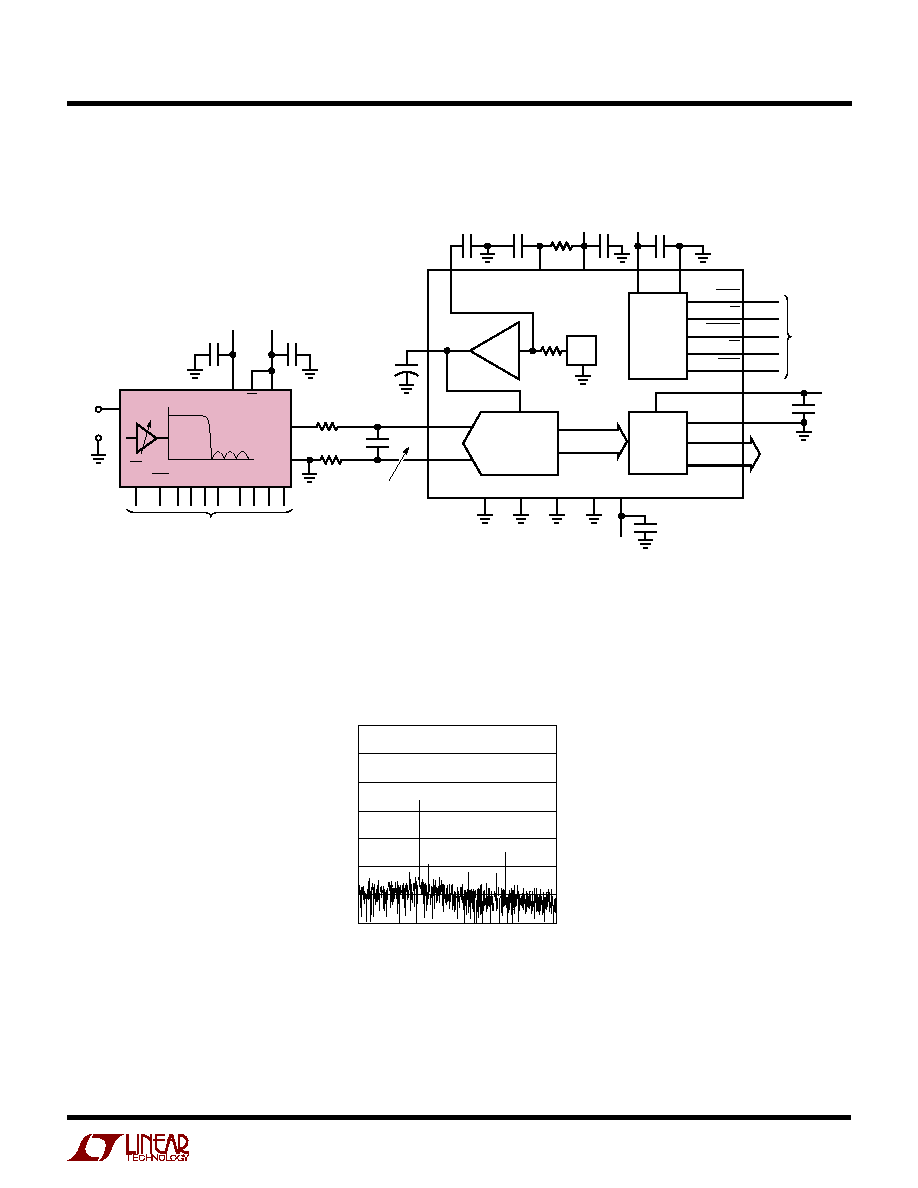
BLOCK DIAGRA
W
G3
AGND
SHUTDOWN
SWITCH
SHUTDOWN
SWITCH
R
V
≠
V
+
V
+
IN
V
≠
EN
G2
G1
G0
F3
CMOS LATCH
VARIABLE
GAIN
AMPLIFIER
F2
F1
F0
1564 F03
CS/HOLD
RST
OUT
PROGRAMMABLE FILTER
R
Figure 3. Block Diagram
9
LTC1564
Functional Description
The LTC1564 is a self-contained, continuous time, vari-
able gain, high order analog lowpass filter. The gain
magnitude between IN and OUT pins is approximately
constant for signal frequency components up to the cutoff
frequency f
C
and falls off rapidly for frequencies above f
C
.
The pins IN, OUT and AGND (analog ground) are the sole
analog signal connections on the LTC1564; the others are
power supplies and digital control inputs to select f
C
(and
to select gain if desired). The f
C
range is 10kHz to 150kHz
in 10kHz steps. The form of the lowpass frequency re-
sponse is an 8-pole elliptic type with two stopband notches
(Figure 4). This response rolls off by approximately 100dB
from f
C
to 2.5f
C
. The LTC1564 is laser trimmed for f
C
accuracy, passband ripple, gain and offset. It delivers a
combination of 100+dB stopband attenuation, 100+dB
signal-to-noise ratio (SNR) and 100+kHz f
C
.
Digital Control
Logic levels for the LTC1564 digital inputs are nominally
rail-to-rail CMOS. (Logic 1 is V
+
, logic 0 is V
≠
or alterna-
tively 0V with
±
5V supplies). The part is tested with 10%
and 90% of full excursion on the inputs, thus
±
1.08V at
±
1.35V supplies,
±
1.9V at
±
2.375V and 0.5V and 4.5V at
±
5V.
The f
C
and gain settings are always controlled by the out-
put of an on-chip CMOS latch. Inputs to this latch are the
pins F3 through F0, G3 through G0, the latch-enable con-
trol CS/HOLD and the asynchronous reset input RST. A
logic-0 input to CS/HOLD makes the latch transparent so
that the F and G input pins pass directly to the latch outputs
and therefore control the filter directly. Raising CS/HOLD
to logic 1 freezes the latch's output so that the F and G input
pins have no effect. Logic 0 at the RST input at any time
resets the latch outputs to all zeros. The all-zero state, in
turn, imposes a mute mode with zero gain and low output
noise if the filter is powered on (EN = 0). The all-zeros
condition will persist until RST is returned to logic 1, non-
zero F and G inputs are set up and the latch outputs are
updated by CS/HOLD = 0. EN is a chip-enable input caus-
ing a shutdown state. Specific details on the digital con-
trols appear in the Pin Functions section of this data sheet.
Floatable Digital Inputs
Every digital input of the LTC1564 includes a small current
source (roughly 10
µ
A) to float the CMOS input to V
+
or V
≠
potential if the pin is unconnected. Table 4 summarizes the
open-circuit default levels.
Table 4. Open-Circuit Default Input Levels
INPUT
FLOATING LOGIC LEVEL
EFFECT
EN
1
Shutdown State
CS/HOLD
0
F and G Pins Enabled
RST
1
Latch Not Reset
F3 F2 F1 F0
0 0 1 0
f
C
= 20kHz
G3 G2 G1 G0
0 0 0 0
Unity Passband Gain
Note particularly that the pull-up current source at the EN
pin forces the LTC1564 to the shutdown state if this pin is
left open. Therefore the user
must connect EN deliberately
to a logic-0 level (V
≠
, or optionally 0V with
±
5V supplies)
for normal filter operation. The other digital inputs float to
APPLICATIO S I FOR ATIO
W
U
U
U
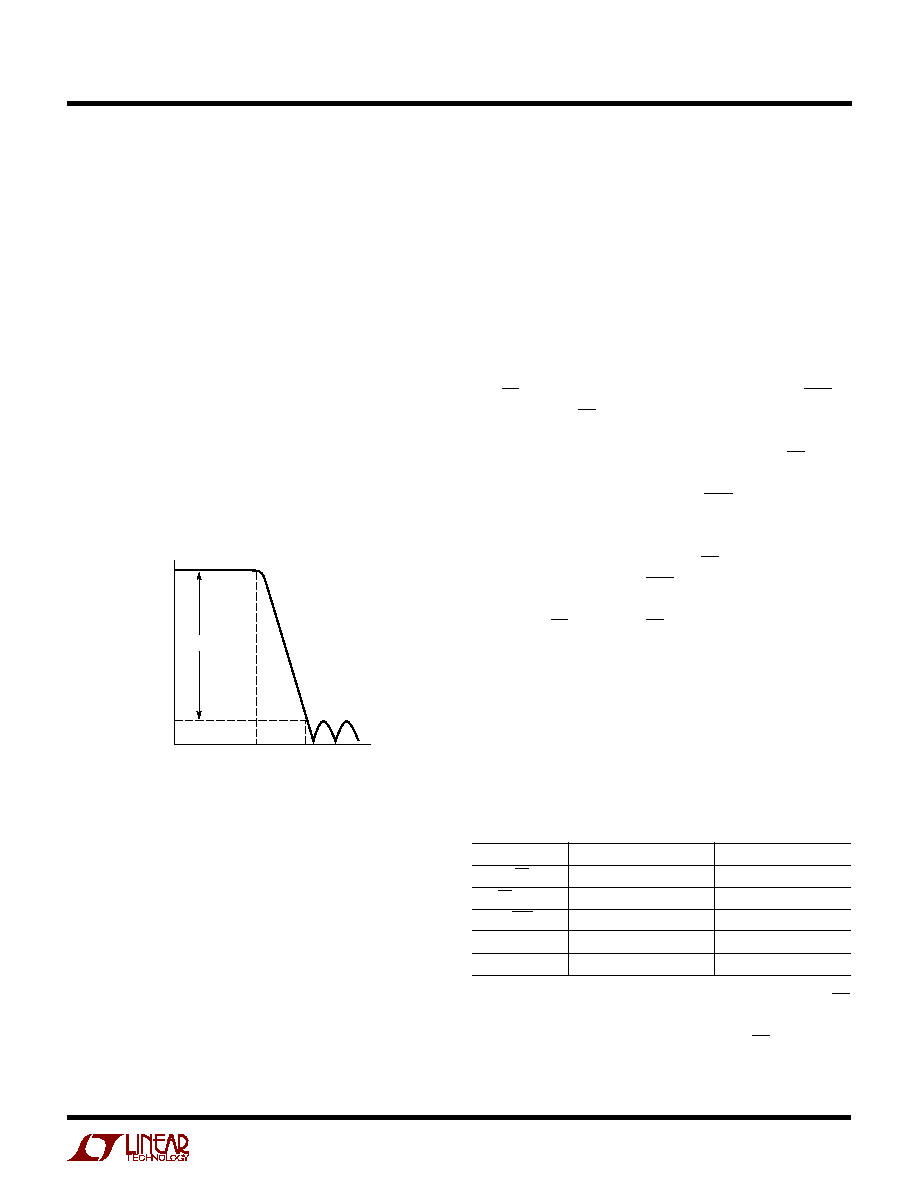
100dB
FREQUENCY (Hz)
GAIN (dB)
f
C
2.5f
C
1564 F04
Figure 4. General Shape of Frequency Response
Figure 3 is a block diagram showing analog signal path,
digital control latch, and analog ground (AGND) circuitry.
A proprietary active-RC architecture filters the analog
signal. This architecture limits internal noise sources to
near the fundamental "kT/C" bounds for a filter of this
order and power consumption. The variable gain capability
at the input is an integral part of the filter, and allows
boosting of low level input signals with little increase in
output referred noise. This permits the input noise floor to
drop steadily with increasing gain, enhancing the SNR at
lower signal levels. Such a property is difficult to achieve
in practice by combining separate variable gain amplifier
and filter circuits.

10
LTC1564
APPLICATIO S I FOR ATIO
W
U
U
U
levels that program the part for enabled F and G pins
(CS/HOLD = 0), 20kHz f
C
and unity passband gain. There-
fore six connections (power pins, EN to logic 0, AGND, IN
and OUT) are enough to set up a working 20kHz lowpass
filter, and additional pins can be connected as necessary
to select different f
C
or gain.
This feature of floatable logic inputs is intended for rapid
prototyping and experimentation. Floating the logic inputs
is not recommended for production designs because,
depending on construction details, the high impedances
of these inputs may permit unwanted interference cou-
pling and consequent erroneous digital inputs to the
LTC1564.
Also, it may be necessary to consider the effect of the pull-
up and pull-down current sources on the logic that drives
the LTC1564. In particular, if the LTC1564 operates from
±
5V but receives digital inputs from logic using 5V and 0V,
CMOS logic levels will be compatible but the possibility
exists of the LTC1564 pulling current out of the driving logic
at those LTC1564 inputs that are capable of floating to logic
0. That is because the small current sources at these in-
puts return to V
≠
, not to 0V. If the driving logic presents a
high impedance or three-state output, the LTC1564's in-
put current may pull this output below 0V, although the
current is limited to about 10
µ
A. The system designer
should be aware of this possibility and ensure that any such
current flow is compatible with the driving logic.
Mute State
The Mute mode keeps the filter powered as in normal
filtering but "turns off" the signal path for minimal signal
transmission (approximately ≠100dB) and reduced out-
put noise. This feature may be useful for gating a signal
source on and off, or for system calibration procedures.
Note however that the DC output in the Mute state may
shift by some millivolts compared to normal filtering
because the internal signal path changes. Recovery from
Mute, like other transient responses in a filter, proceeds at
the time scale of the filter's pole-zero time constants and
therefore is faster at the higher f
C
settings (that is, at the
higher F codes).
The LTC1564 enters the Mute state when the F bits at the
latch output (Figure 3) become 0000. (It can be remem-
bered as a "zero-bandwidth" frequency setting.) This is
achieved either by presenting a 0000 code to the F inputs
and lowering the CS/HOLD input to enable the latch, or
alternatively at any time by lowering RST, which immedi-
ately resets the latch contents to all zeroes. Such a reset
also occurs normally at the application of power, unless
CS/HOLD is low and a nonzero pattern at the F inputs
overrides the brief power-on reset. In the Mute state, the
G gain-control inputs have no effect.
Output noise in Mute is largely thermal and wideband
(unlike in normal filtering, where the filter's response
affects the noise spectrum). Typical Mute-state output
noise is 5.4
µ
V
RMS
in 200kHz measurement bandwidth
and less than 3
µ
V
RMS
in 40kHz bandwidth. It has occa-
sionally happened elsewhere in the electronics industry
that someone would characterize a circuit or system by
comparing its output level in normal operation to the noise
level in a Mute state as though this were a normal signal-
to-noise ratio (SNR), which it is not, because this signal
and noise exist only at different times. A scrupulous name
for such a measure is SMR, signal-to-mute ratio. Accord-
ingly in a 40kHz bandwidth, the LTC1564 can exhibit an
SMR exceeding 120dB.
Construction and Instrumentation Cautions
Electrically clean construction is important in applications
seeking the full dynamic range or high stopband rejection
of the LTC1564. Short, direct wiring will minimize parasitic
capacitance and inductance. High quality supply bypass
capacitors of 0.1
µ
F near the chip provide good decoupling
from a clean, low inductance power source. But several
inches of wire (i.e., a few microhenrys of inductance) from
the power supplies, unless decoupled by substantial ca-
pacitance (
10
µ
F) near the chip, can cause a high-Q LC
resonance in the hundreds of kHz in the chip's supplies or
ground reference. This may impair stopband rejection and
other specifications at those frequencies. In stringent filter
applications we have often found that a compact, carefully
laid out printed circuit board with good ground plane
makes a difference in both stopband rejection and distor-
tion. Finally, equipment to measure filter performance can
itself introduce distortion or noise floors. Checking for
these limits with a wire replacing the filter is a prudent
routine procedure.
11
LTC1564
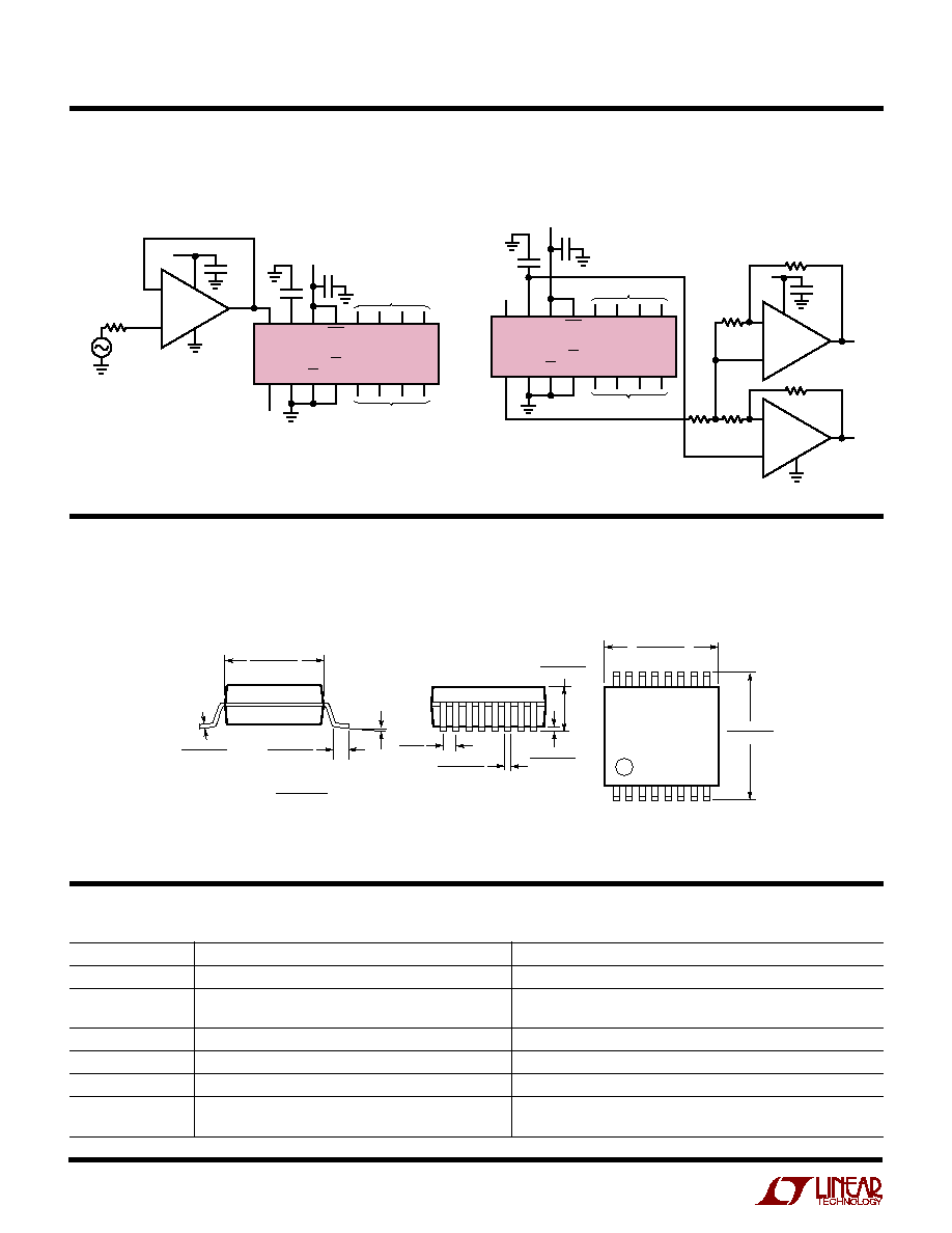
TYPICAL APPLICATIO S
U
16-Bit Output, Sampling Rate to 500ksps, Analog Bandwidth to 150kHz, Gain to 24dB.
(For More Information, See
Linear Technology Magazine, May 2001)
2-Chip Flexible DSP Front End with Amplification,
Antialias Filtering and A/D Conversion
Boosting a 100mV
RMS
Input Signal to Nearly Fill the Input Range of the LTC1608 ADC. Input Frequency of 40kHz,
LTC1608 f
SAMPLE
= 204.8ksps, LTC1564 is Set for f
C
= 50kHz and Gain of 16 (F = 0101, G = 1111). Measured THD
is 86dB, HD
2
= ≠ 88dB, SNR = 85dB with 100mV
RMS
Input. Dynamic Range of Approximately 115dB
4096-Point FFT Spectrum
with Low Level Input
FREQUENCY (kHz)
0
≠60
≠40
0
76.8
1564 TA04
≠80
≠100
25.6
51.2
102.4
≠120
≠140
≠20
AMPLITUDE (dB)
2.2
µ
F
1
µ
F
1
µ
F
10
22
µ
F
4
6
DIFFERENTIAL
ANALOG INPUT
±
2.5V
REFCOMP
CONTROL
LOGIC
AND
TIMING
B15 TO B0
16-BIT
SAMPLING
ADC
≠
+
1
µ
F
5V OR
3V
µ
P
CONTROL
LINES
D15 TO D0
OUTPUT
BUFFERS
16-BIT
PARALLEL
BUS
11 TO 26
OGND
OV
DD
28
1564 TA03
29
1
2
A
IN
+
A
IN
≠
SHDN
CS
CONVST
RD
BUSY
33
32
31
30
27
7.5k
LTC1608
3
36
35
10
9
5V
5V
AV
DD
AV
DD
DV
DD
DGND
V
REF
8
AGND
AGND
7
AGND
5
AGND
34
≠5V
V
SS
1
µ
F
2.5V
REF
1
µ
F
1.75X
+
V
+
EN V
≠
OUT
AGND
IN
16
CS/
HOLD RST
F
4
5 6 7 8
9 10 11 12
15
1
2
3
14
13
G
LTC1564
5V
≠5V
0.1
µ
F
0.1
µ
F
249
1% METAL FILM
249
1% METAL FILM
C1*
FILTER CONTROL
ANTIALIAS FILTER/AMP
ADC
A
V
f
C
INPUT
+
≠
*C1 IS A 1000pF NPO, SURFACE MOUNT DEVICE
PLACE AS CLOSE AS POSSIBLE TO THE LTC1608 INPUT PINS
A
V
Information furnished by Linear Technology Corporation is believed to be accurate and reliable.
However, no responsibility is assumed for its use. Linear Technology Corporation makes no represen-
tation that the interconnection of its circuits as described herein will not infringe on existing patent rights.
12
LTC1564
©
LINEAR TECHNOLOGY CORPORATION 2001
1564f LT/TP 0401 4K ∑ PRINTED IN USA
Linear Technology Corporation
1630 McCarthy Blvd., Milpitas, CA 95035-7417
(408) 432-1900
q
FAX: (408) 434-0507
q
www.linear-tech.com
RELATED PARTS
U
PACKAGE DESCRIPTIO
G Package
16-Lead Plastic SSOP (5.3mm)
(Reference LTC DWG # 05-08-1640)
TYPICAL APPLICATIO S
U
IN AGND V
+
RST G3
LTC1564
G2
G1
G0
OUT V
≠
1
2
3
4
5
6
7
1564 TA05
8
16
6
7
2
3
R
SOURCE
10k
4
V
SOURCE
V
IN
15
14
13
12
11
GAIN CODE
FREQUENCY CODE
V
+
SUPPLY FROM 2.7V TO 10.5V
TIE F AND G PINS TO V
+
OR GROUND
TO SET FREQUENCY AND GAIN
0.1
µ
F
1
µ
F
V
+
0.1
µ
F
V
+
10
9
EN
CS/
HOLD F3
F2
F1
F0
V
OUT
+
≠
+
LT1677
Single Supply, Very Low Noise Input Buffer for High Impedance
Source Driving the Input of LTC1564
Single Supply Differential Output Driver
IN AGND V
+
RST G3
LTC1564
G2
G1
G0
OUT V
≠
1
2
3
4
5
6
7
1564 TA06
8
2.49k
16
15
14
13
12
11
GAIN CODE
FREQUENCY CODE
V
+
SUPPLY FROM 4.5V TO 10.5V
TIE F AND G PINS TO V
+
OR GROUND
TO SET FREQUENCY AND GAIN.
OUTPUTS DRIVE 100
/1000pF LOADS
0.1
µ
F
1
µ
F
V
IN
V
+
10
9
EN
CS/
HOLD F3
F2
F1
F0
2.49k
6
5
4
7
V
OUT
≠
2.49k
2.49k
≠
+
1/2 LT1813
2
8
V
+
3
1
0.1
µ
F
V
OUT
+
2.49k
≠
+
1/2 LT1813
G16 SSOP 0401
.13 ≠ .22
(.005 ≠ .009)
MILLIMETERS
(INCHES)
0
∞
≠ 8
∞
.55 ≠ .95
(.022 ≠ .037)
5.20 ≠ 5.38**
(.205 ≠ .212)
7.65 ≠ 7.90
(.301 ≠ .311)
1
2 3
4
5
6 7 8
6.07 ≠ 6.33*
(.239 ≠ .249)
14 13 12 11 10 9
15
16
1.73 ≠ 1.99
(.068 ≠ .078)
.05 ≠ .21
(.002 ≠ .008)
.65
(.0256)
BSC
.25 ≠ .38
(.010 ≠ .015)
1. CONTROLLING DIMENSION: MILLIMETERS
2. DIMENSIONS ARE IN
*
**
DIMENSIONS DO NOT INCLUDE MOLD FLASH. MOLD FLASH
SHALL NOT EXCEED .152mm (.006") PER SIDE
DIMENSIONS DO NOT INCLUDE INTERLEAD FLASH. INTERLEAD
FLASH SHALL NOT EXCEED .254mm (.010") PER SIDE
PART NUMBER
DESCRIPTION
COMMENTS
LTC1560-1
1MHz/500kHz Continuous Time, Lowpass Elliptic Filter
f
CUTTOFF
= 500kHz or 1MHz
LTC1562/LTC1562-2
Universal 8th Order Active RC Filters
f
CUTOFF(MAX)
= 150kHz (LTC1562),
f
CUTOFF(MAX)
= 300kHz (LTC1562-2)
LTC1563-2/LTC1563-3 4th Order Active RC Lowpass Filters
f
CUTOFF(MAX)
= 256kHz
LTC1565-31
650kHz Continuous Time, Linear Phase Lowpass Filter
7th Order, Differential Inputs and Outputs
LTC1566-1
2.3MHz Continuous Time Lowpass Filter
7th Order, Differential Input and Outputs
LTC1569-6/LTC1569-7 Self Clocked, 10th Order Linear Phase Lowpass Filters
f
CLK
/f
CUTOFF
= 64/1, f
CUTOFF(MAX)
= 75kHz (LTC1569-6),
f
CLK
/f
CUTOFF
= 32/1, f
CUTOFF(MAX)
= 300kHz (LTC1569-7)